|
Summarize:
Applied programmable chip , up to 450MHz working frequency, offer
strong ability and can through the codes to improve the performance.
Multiple modes built in for users select , it is better choice of
DIYers.
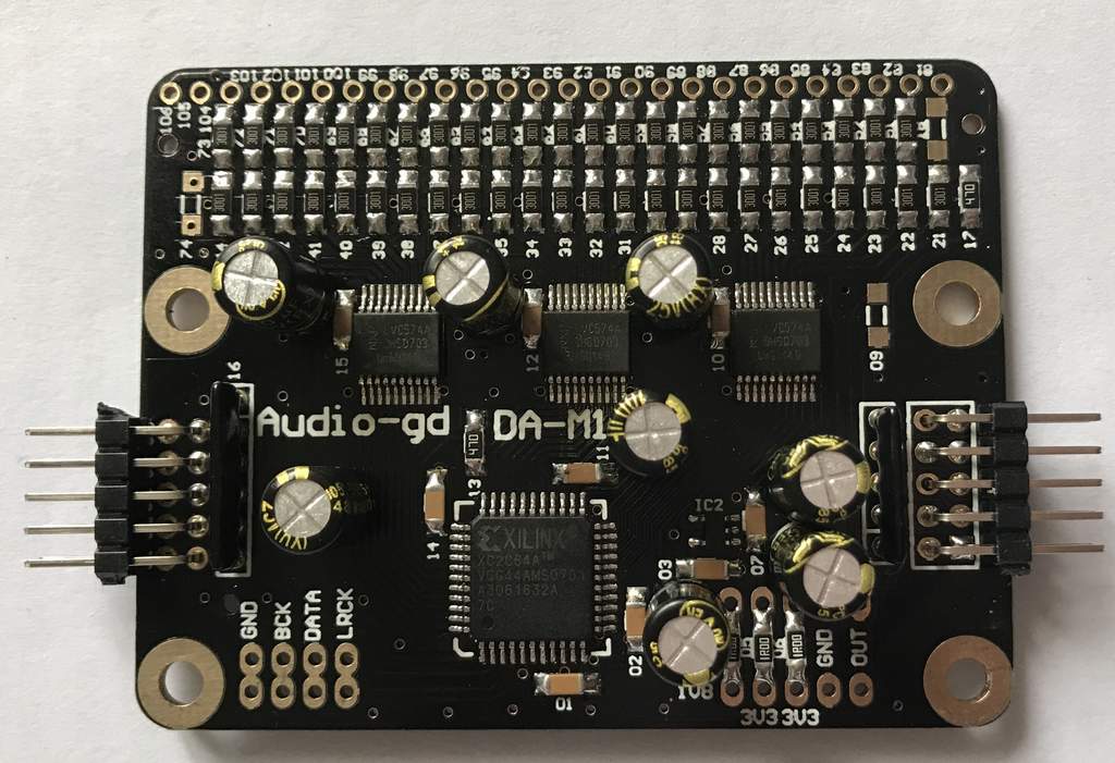
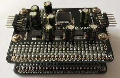
1, It can setting working
either NOS mode (IIS input) and after digital filter ( Right
Justified ) so it can easy for DIY a new DAC or replace the DA chips
in the original DAC .
2, It can setting working
either left and right channels, the two DA modules just want to
connect same IIS input signal and can working as stereo DAC without
external process .
3, It can setting either invent
and non invent , four pcs modules can connect same IIS input signal
and working as balanced stereo DAC without external process .
4, It can setting working in Pull / Push mode as the PCM1704
technology, two module working for one output , one for the positive
wave , another for the negative wave , refuse the zero distortion .
Even though without Pull/ Push mode, only one pc working, the zero
distortion is very low.
Support up to 24 BIT / 3072Khz in NOS mode, and 384Khz in 8x
oversampling mode.
Low Power Consumption, only need +3.3V (+/- 5%) / 30mA power.
|
|
Example for applied:
Please note:
1, There is already built in 1.8V PSU, so the on board 1.8V pin
can't connect to external power. If customer want to power supply by
external power, must remove the on board 1.8V PSU.
2, The product for DIY, before shipping ,we had the full check, but
it may damage by wrong power connect or other case, so it had not
warranty after shipping .
3, It working with 64 BCLK format data.
The most simply USB NOS DAC circuit diagram (It had applied
the USB power supply so the output voltage level is slight low)
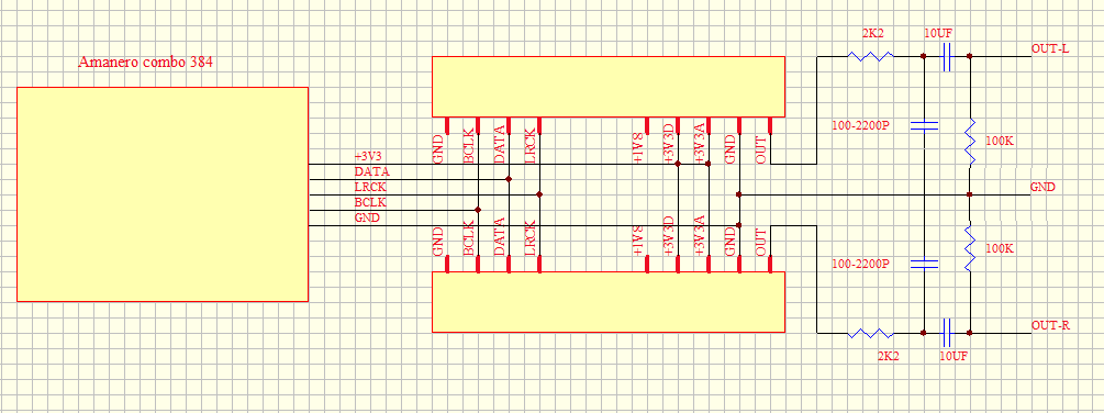
Standard stereo NOS dac circuit diagram .
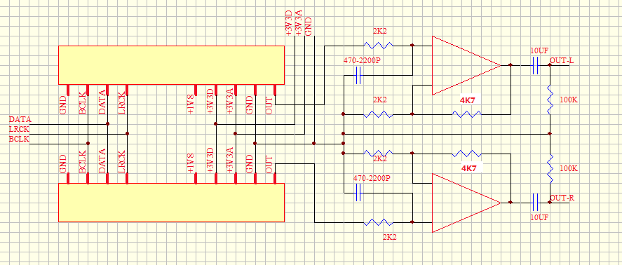
One channel Pull/ push mode NOS dac
circuit diagram .
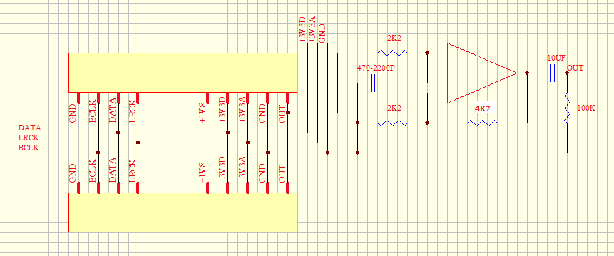
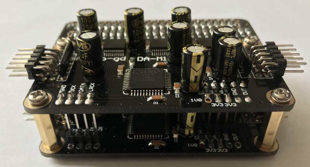
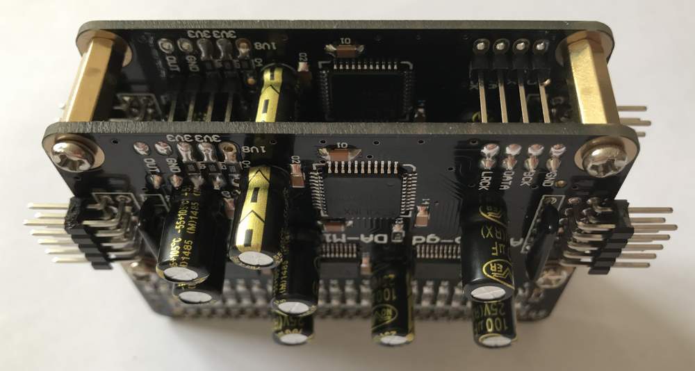
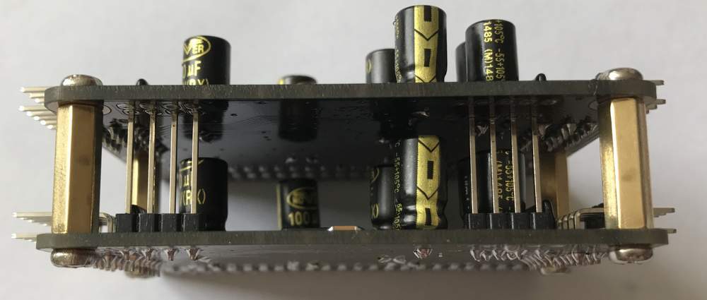
Recommend one channel balance assemble guide
(we are not recommend assemble two channels as below):

Recommend one channel Push/ Pull assemble
guide (One channel balance Push/ pull can assemble 4 pcs together
but customer want to buy the longer pins or enough length copper
wires for connect them):
Setting guide:
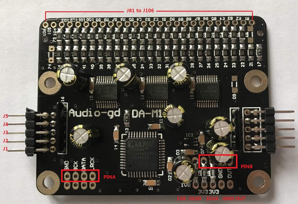
J1 :Two pcs module working in Push/ pull mode, must push into
a jumper.
J2 :Two pcs module working in Push/ pull mode, the positive
wave module without jumper but the negative wave module want to push
into a jumper.
J3 :Build the NOS DAC, left channel without jumper but the
right channel with the jumper.
J4 :Build the NOS DAC and with IIS input, without jumper but
build the oversampling DAC with Right Justified input must push into
a jumper.
J5 :Without jumper for non invert output, with jumper for
invert output.
Setting examples :
2 pcs modules build the NOS DAC with IIS input:
Left channel module without any jumper, but Right channel with a
jumper on J3.
4 pcs modules built the NOS DAC with IIS input and
working with Push / pull mode : Every channel had 2 pcs modules
and the J1 must with jumpers , 1 pc module must push into a jumper
to J2 for setting working for negative wave .Another module without
jumper on J2 for working as positive wave . Every channel had
connect J81 to J106 (The J104 and J105 can short by tins), PINA and PINB. The input signal and output
signal just want to connect from one module.
4 pcs modules built the balance DAC : Every
channels had 2 pcs modules , one of them push into a jumper on J5
for setting as cold output, another without jumper on J5 for hot
output.
Replace the DA chip in the original DAC : If the
DAC had built in digital filter, please confirm its output format is
Right Justified . The left module connect the DOL , WCK and BCK from
digital filter and the right channel connect the DOR, WCK and BCK,
and both modules had jumper on J4 .
Tips:
The module had separate digital and analog power input,
it is better had separate power supply , and the power had good
quality .
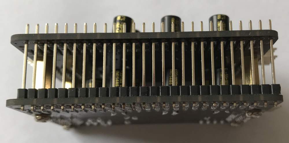
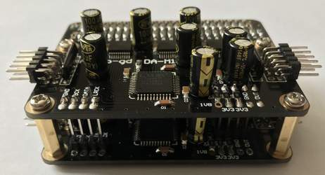
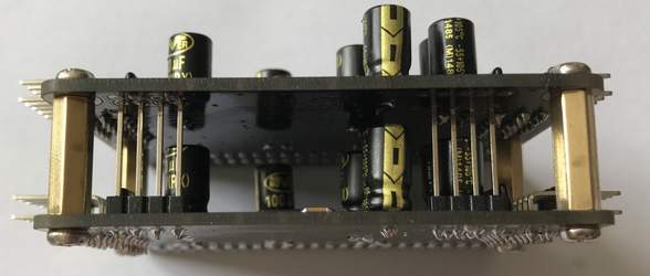
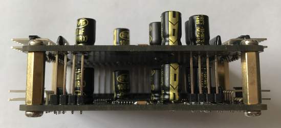
While 2 pcs module working with Push / Pull or balance
modes, assemble them together by 15MM copper pillars, solder the
PINA and PINB together by 21MM copper pins , the power supply,
signal input and output just want to connect on one module.
The module had the DC offset , customer want to use the
couple cap, or the DAC analog filter output had the couple caps or
DC serve design. For the balance DAC design, the proper design can
remove the DC offset in the analog filter amp output , without
couple caps or DC serve design .
The module had better with over 10K ohm impedance load .
|