|
Price:
USD879( Exclude shipping cost)
Two chassis versions available,
customer must inform while place the order ,otherwise we ship the
edition randomly:
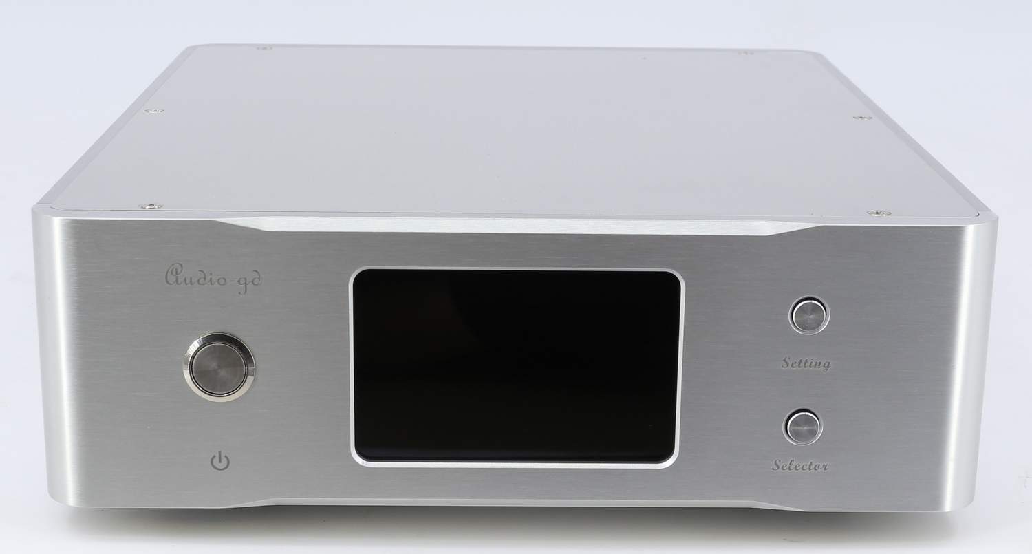
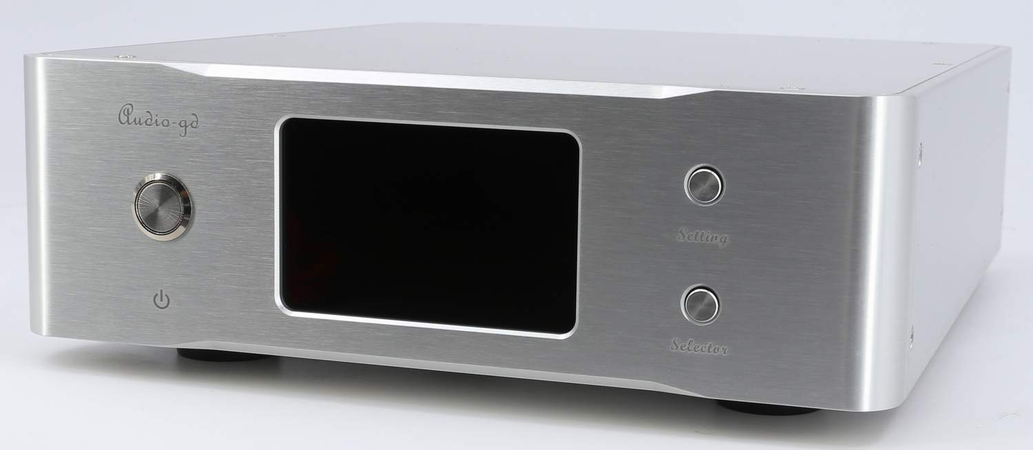
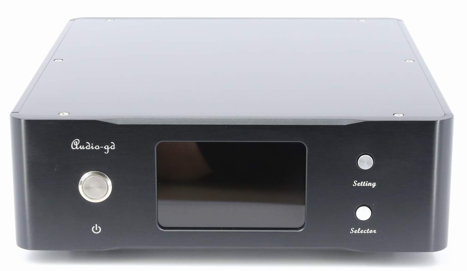
R-1 MK3 Black
R-1 MK3 Silver
Please send your address, name
to audio-gd@vip.163.com
get the quote.
Click to download the
driver of
Amanero
combo 384
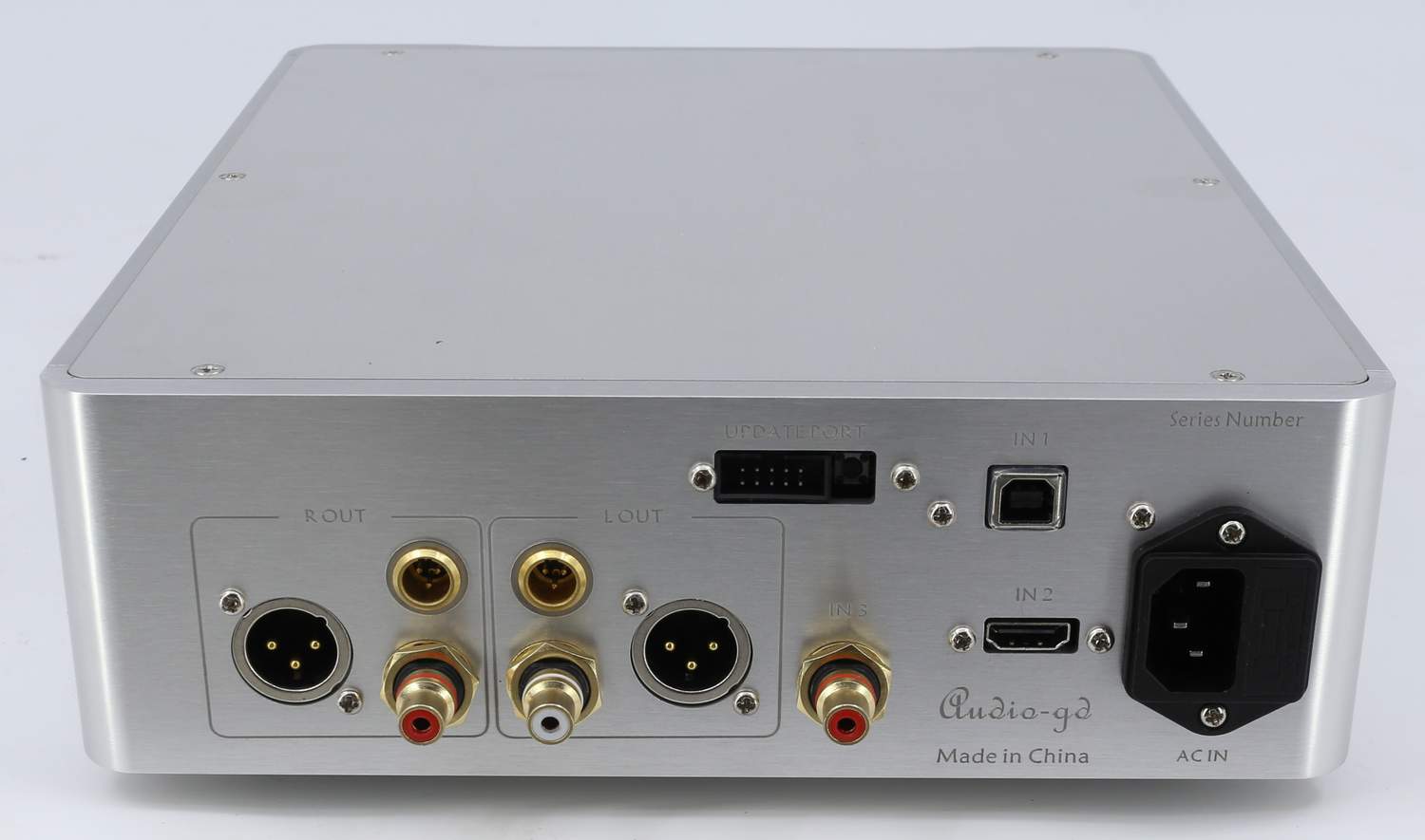
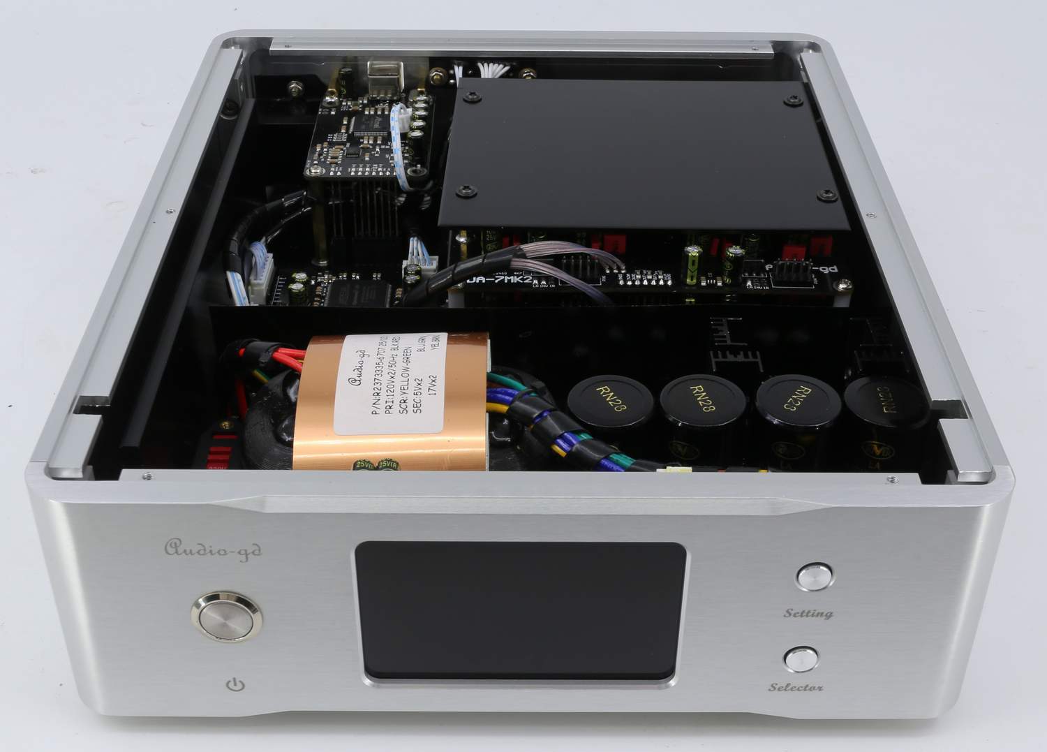
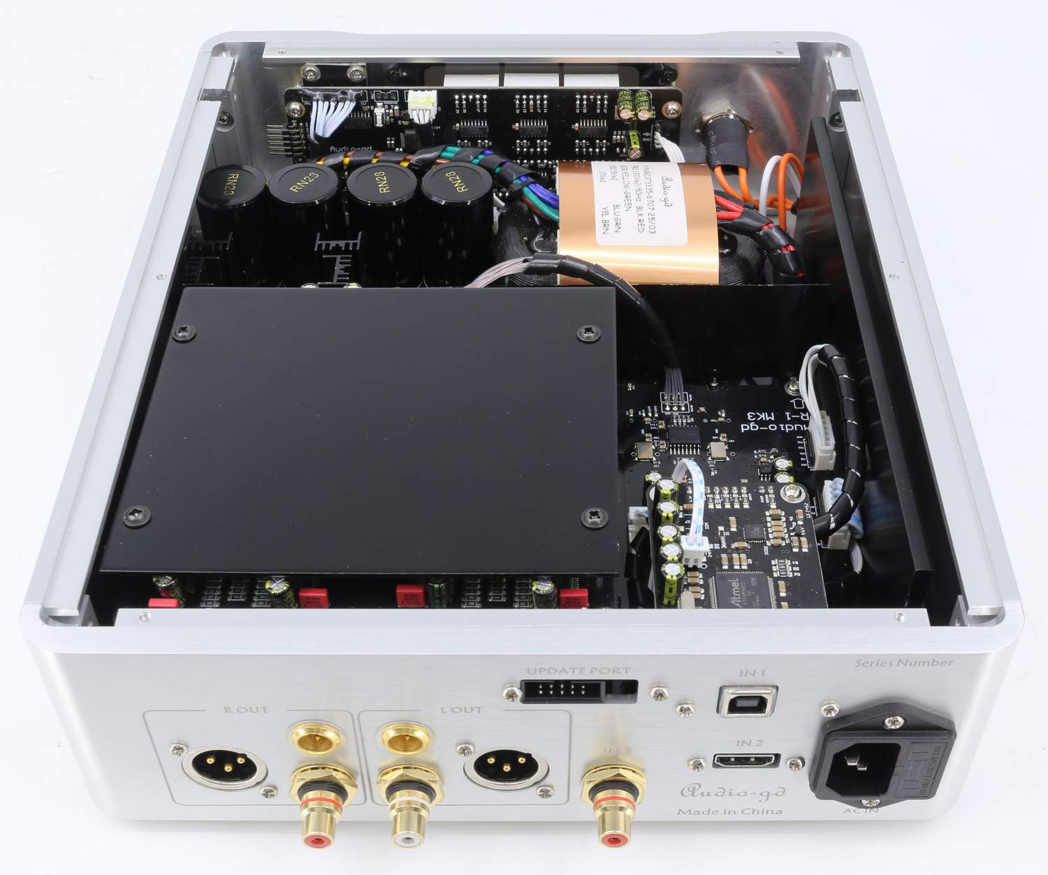
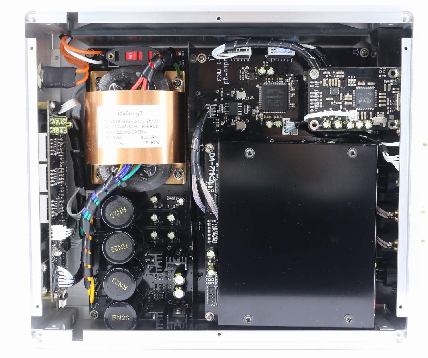
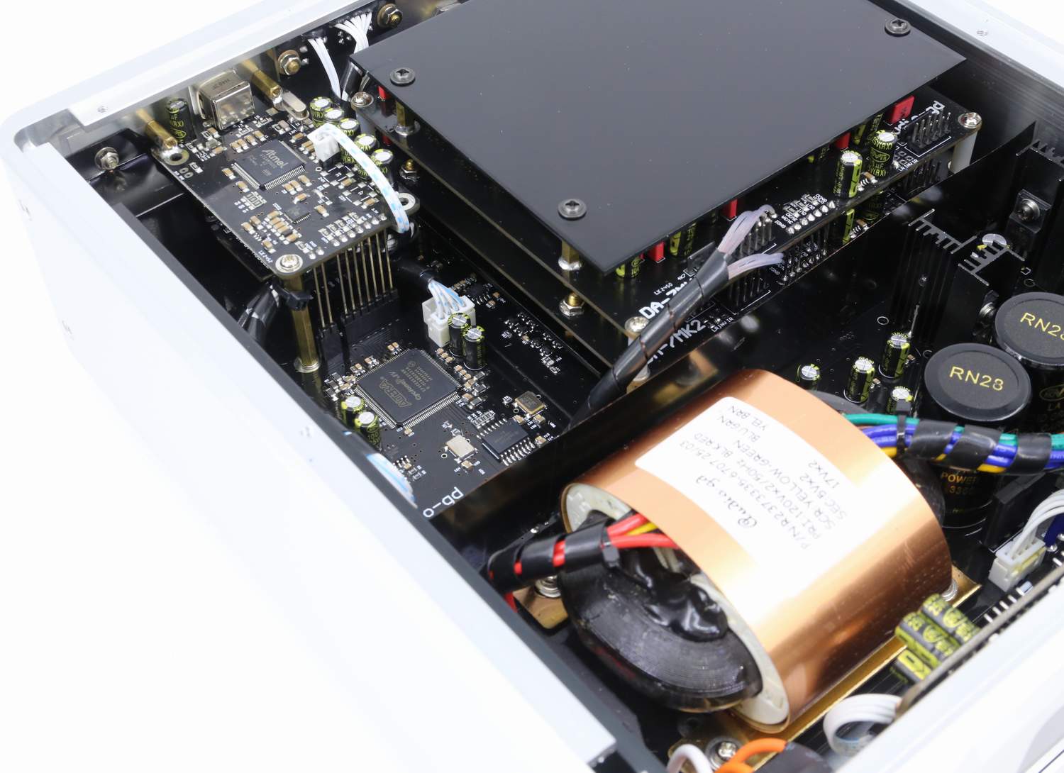
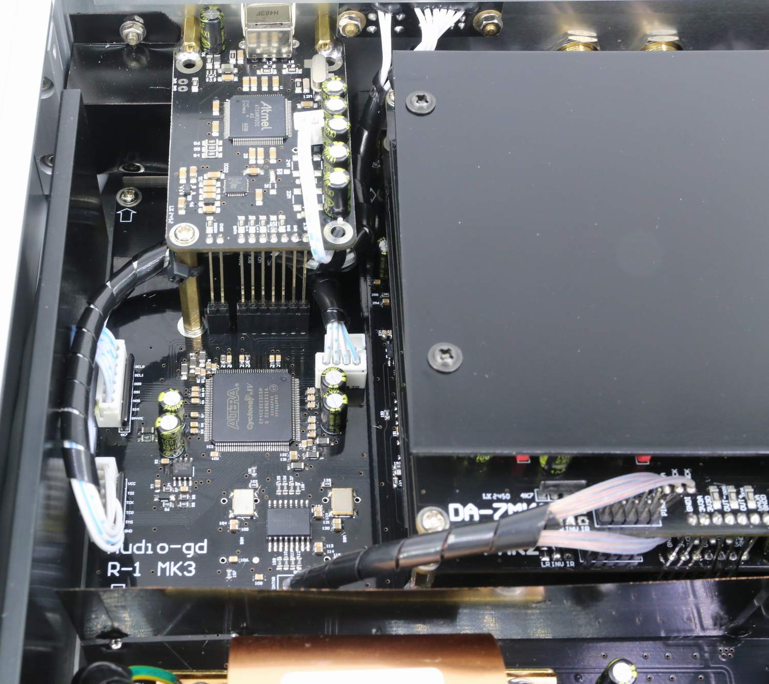
R-1 MK3 feature:
1, Built in isolator for total isolate
of the all inputs include USB,HDMI and spdif inputs , and the FPGA
processor to the analog parts .
2, Fully balance discrete transistors
analog part design.
3, R core transformer
power supply separately, built in 7 ground ultra speed linear PSUs
and two ground pure class A PSUs
5, Real balance DAC design ,built in 4 group
fully discrete real balanced DSD native decoders , 8 group fully
discrete R-2R PCM decoders and 32bit / PCM384K /DSD512 asynchronous
transfer Amanero 384 .
6, USB transmit the IIS signal to the FPGA processor and receive the
clock signal from the FPGA processor, the USB interface without on
board data clocks, the signal transmit is much exact, the sound
quality get the much improve .
7, The FPGA process data in the parallel mode.
The IIS data is series transmit
mode, every data must need one clock cycle to process or transmit,
one frame data ( Include L and R data) must need 64 clock cycle to
process or transmit, so the data has effect by the 64 clock cycles.
But the parallel data process
and transmit mode only need one clock cycle can finish the one frame
data process
and transmit, that can avoid the effect of clock stability .
The IIS input (Include USB and HDMI-IIS) has recombine become dual
32bit parallel data once input , and the SPDIF input after decoder, has
recombine become dual 24bit parallel data, and the DSD input has
recombine become dual 64bit parallel data once input.
The parallel process and
transmit mode can improve the sound quality on the transparency and
detail but still analog.
8, Full new configuration clock
manage design built
in, improved on the clock timing.
9, DSD asynchronous clock technology
has apply that improves the sound quality obviously.
10, DOP support from SPDIF input .
The advantages and disadvantages
of R-2R DAC:
Advantages:
1, R-2R will not convert the
clock signal to the output signal.
2, R-2R is not sensitive to
jitter but Delta-Sigma is quite sensitive.
3, The output signal level of
R-2R is more accurate than Delta-Sigma.
Disadvantages:
1, R2R's harmonic distortion
can be quite low but not as low as the ES9038 PRO (Delta-Sigma)
harmonic distortion.
2, The accuracy and inherent
glitches of resistor ladders are not easy to deal with.
R-2R design popular in the market:
Whether it is DIY kits or
factory products, R-2R has become popular.
In the low-cost DIY kit market,
the usual design is based on the old MSB technology, but only retain
the signal conversion part and discard the exquisite design of the
original product.
This design uses data serial input to
a shift register IC to convert data to an analog signal. It is not
able to solve the technical problem of R-2R at all. The performance
of this design is completely dependent on the accuracy of the ladder
resistances.
The
factory products in the high-end market use quite complex technology
to solve the problems of R-2R, in order to achieve high performance
and sound quality. Some manufacturers use the serial control mode of
the shift register IC.
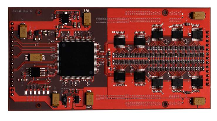
The design in the figure
below uses an FPGA to control the step resistance switching in
parallel. With the parallel control mode, the step resistance switch
of each bit is individually controlled, so it has ultra-high speed
(parallel mode only needs 1 clock cycle to output all bits, serial
mode requires at least 8 to 24 clock cycles) to send or update the
data, and can correct the data at any time to achieve an output
signal with low-distortion characteristics, and solve the problems
caused by resistance tolerances and switching glitches.
The accuracy of the step
resistance:
Many people only care
about the accuracy of the step resistances because they think that
R-2R depends essentially on the accuracy of the resistance.
Nowadays, 24 bit is a standard, but
can the precision of manufactured resistors reach 24 bit? Even with
only 16 bits, the accuracy requirement is 1/66536, and so 0.1%
(1/1000) of accuracy is completely inadequate. In fact, 0.01%
(1/10000) would still fail to meet the 16-bit requirement, let alone
24 bits.
Therefore, lowering accuracy of
the resistance is not enough to solve the problem. If there were
0.00001% resistors available on the market, it would meet the
requirement of 24 bits, but the inherent resistance of the switching
devices would completely wipe out this super high accuracy
advantage.
We need to solve the
problem technically, not just improve the accuracy of the
resistance. But we still use ultra-high precision resistors in our
products.
Importunacy of the FPGA/CPLD:
On important thing to
underline about the FPGA/CPLDs is that they are programmable logic
array devices. Nowadays, FPGAs have been used in many high-end DAC
products, such as the popular ROCKNA WAVEDREAM DAC.
Since 2008, we have used
FPGA designs in DAC products. This machine is composed of one FPGA
and 5 CPLDs at the heart of digital processing.
The hardware layout
inside the FPGA can be designed and arranged through software,
therefore the hardware can be upgraded through software updates.
As a benefit, this
design has a high degree of flexibility. It allows improving sound
quality, adding functions, and keeping the product up-to-date, all
through software (firmware) updates.
Responsibilities hor the FPGA/CPLDs:
1. the FPGA implements a
high-performance SPDIF demodulator (instead of using low-performance
SPDIF demodulator chips such as DIR9001, WM8805, AK411X, etc...).
2. Combining clocking and FIFO
technology to output data, it can be accurately synchronized to the
clock, and thus reject jitter.
3. Built-in 2X, 4X and 8X
digital filters and different NOS modes allow users to choose the
tone that best suits their personal taste.
4. Simulate the tonality of
vinyl disc playback through a unique design.
Fully
discrete output stage:
The last stage in the
signal journey is the analog output stage, and the output stage has
a decisive influence on the sound quality of the DAC.
No matter how excellent
digital circuit design is, without an excellent analog output stage
design, the sound quality will become extremely ordinary.
The analog output stage
is directly connected behind the DA 7 module, using only
through-hole components (not SMD).
The high-speed ACSS
amplifier is used for signal amplification and processing. The ACSS
amplifier is designed without negative feedback and works in the
current signal mode. It does not have to repeatedly transform the
signal between current and voltage like other designs.
The output buffer stage
is a single-ended pure class-A FET design, and the two groups are
connected in parallel to achieve a lower output impedance. All in
all, the output stage is working in a pure class-A state, with no
negative feedback at all, so that it can reproduce pure and lifelike
sound signals.
The DAC has four
built-in operational amplifiers to serve in the DC servo function,
so that the DAC can work without coupling capacitors, avoiding noise
and coloration. In the whole signal channels following the DA
module, no switching elements are used to achieve the truest and
purest sound quality.
|